Size Standards
(10)-
Starting at €666.90 €793.61
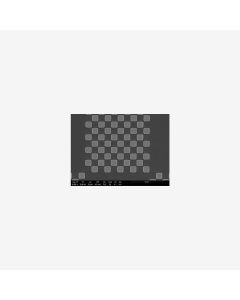
The Checkerboard Calibration Standard is a precise instrument for magnification and image calibration of Scanning Electron Microscopes (SEM). It features a complex checkerboard pattern with feature sizes ranging from 1µm to 5mm, fabricated using 60nm thick chromium on a conductive silicon substrate. The standard is suitable for magnifications from 20x to 50,000x with an accuracy of ±0.1% and is NIST traceable. It is designed for both calibration and image distortion checks and is available in various mounting options.Starting at €666.90 €793.61
-
 Art.Nr: GQ-AFM
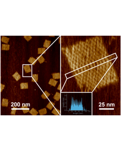
With GATTA‑AFM nanorulers, now adequate test samples are finally available. The GATTA-AFM nanorulers represent accurate and highly parallelized structures and are therefore perfectly suited to optimize and test the resolution of atomic force microscopes.
-
 Art.Nr: TL80069The MAG*I*CAL performs all major TEM calibrations: All TEM magnification ranges, Camera constant, Image Diffraction Pattern Rotation, Directly traceable to a natural constant. Magnification range from 1,000x to 1,000,000x.
 -
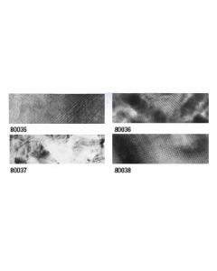 €41.50 €49.39Art.Nr: P80037Since crystal lattice plane spacings are accurately known from x-ray measurements, they provide a good test of microscope stability and a calibration of magnification in the upper range of magnification of the instrument.€41.50 €49.39
 -
€59.50 €70.81Art.Nr: P80036Since crystal lattice plane spacings are accurately known from x-ray measurements, they provide a good test of microscope stability and a calibration of magnification in the upper range of magnification of the instrument.€59.50 €70.81
-
€38.10 €45.34Art.Nr: P80035Since crystal lattice plane spacings are accurately known from x-ray measurements, they provide a good test of microscope stability and a calibration of magnification in the upper range of magnification of the instrument.€38.10 €45.34
-
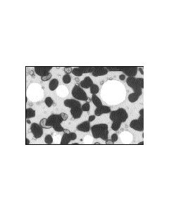 €38.10 €45.34Art.Nr: P80020Evaporated Pt/Ir on Holey carbon film. Holey carbon film support provides holes for ease of focus and astigmatism correction. The dots of evaporated Pt/Ir provide dense particles for resolution checks through the particle seperation test.€38.10 €45.34
 -
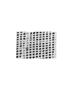 Art.Nr: P79526-10These fine mesh grids are suitable for the low magnification range of a TEM.
 -
€41.50 €49.39Art.Nr: P79525-01These fine mesh grids are suitable for the low magnification range of a TEM. Available as a sandwich in a folding 3.05mm mesh grid.€41.50 €49.39
-
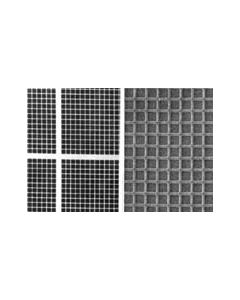 €44.60 €53.07Art.Nr: P79502-01This Test Specimen is made of a 5x5mm square of single crystal silicon. It is photo-etched and the squares repeat every 10µm. The dividing lines are 1.9µm wide. A broader etching line is written every 500µm, which is useful in light microscopy.€44.60 €53.07