Tennant20, ultra high Resolution PE-CVD Coating System
MFTE20
The Tennant20 is an automated PE-CVD system for the production of ultra-thin coatings for SEM, EDX, EBSD, AES and XPS analyses. The rotation-pumped, closed system produces isotropic osmium layers with very small grain sizes and high conductivity. A large number of built-in safety functions ensure safe handling in accordance with laboratory standards.
Take advantage of our free coating service and experience this unknown but proven coating method. Detailed information can be found here.
Product Details
Description
Ultra-thin, conductive, metallic layers can be deposited very easily with the new Tennant20 Osmium Coater. It produces an isotropic, fine-grained coating ideal for non-conductive samples for SEM, EDX, EBSD, AES, XPS analysis.
The product name "Tennant20" derives from the name of the British scientist Smithson Tennant, who discovered Osmium in 1803. He isolated the metal along with iridium in residues of platinum dissolved in aqua regia.
The process:
Plasma-Enhanced-Chemical-Vapor-Deposition (PE-CVD) from OsO4-gas (sublimation source from OsO4 crystals)
The coating:
- Ultra-thin, conductive, pure Os films
- Very fine grain size
- No heat damage
- Isotropic coating
The results:
- Even on samples with a complicated structure, an Os film of 1-10nm thickness fully coats every side of the sample -> very few charging effects in the SEM
- Fine grain size preserves surface structure of samples at high resolution imaging
- Ultra-thin coatings <1nm show very low signal in EDS, EDX, AES, XPS, EBSD analysis
The Safety:
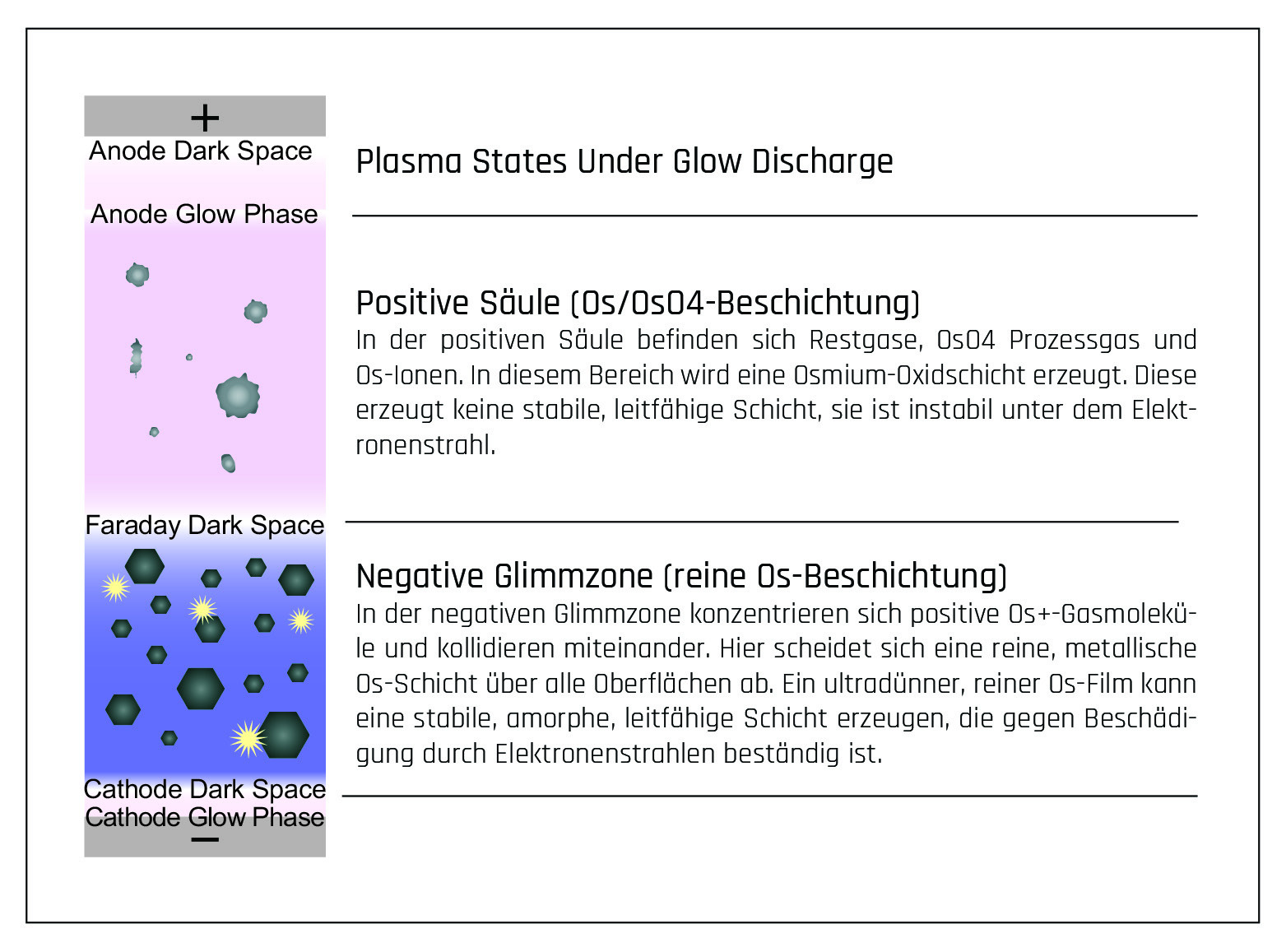
The Osmium coating-process
The Tennant20 osmium coater uses a patented PE-CVD process (plasma-enhanced chemical vapor deposition) to create an ultra-thin yet conductive osmium film with a thickness of less than 1nm up to 30nm.
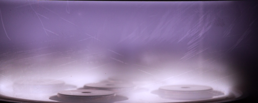
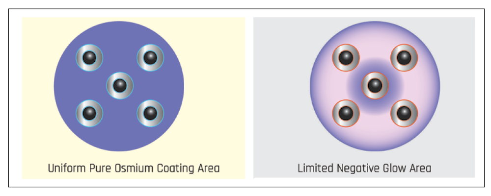
By the plasma CVD method, osmium tetroxide sublimation gas is introduced into the vacuum chamber and plasma is generated by DC glow discharge. During the process, the chamber is separated into two areas: „positive column“ and „negative glow phase“.
 Source: Stefan Diller – Scientific Photography
Height of negative glow phase
The negative glow phase area of conventional electrodes is only 5mm high. An OsO4 coating is formed in the positive column area if a sample is taller than 5mm.
The Tennant20 creates a larger negative glow phase area (20mm high) and larger samples can be coated in superior quality.
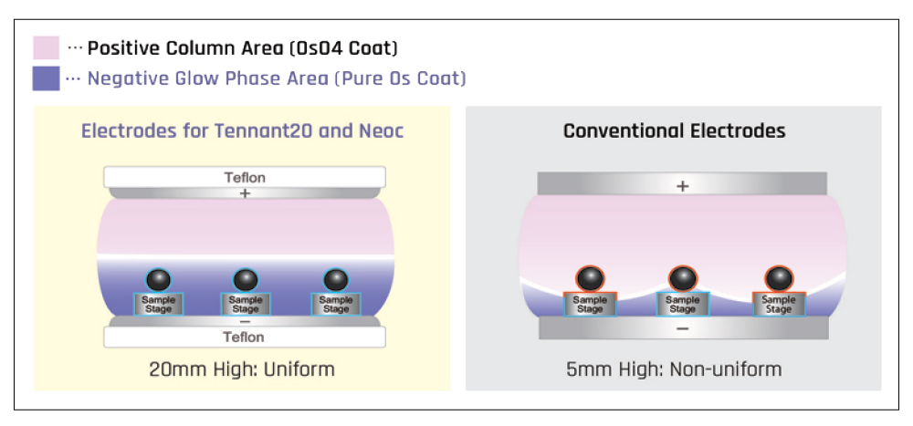
Uniform coating thickness
The coating thickness is non-uniform with conventional parallel plate type electrodes. It is thick at the center and the edge but it is thin in the center ring. The electrodes of the Tennant20 have a special design so that the discharge is not only centered on the edge but shows a uniform negative glow phase in the whole sample holding area.
The Osmium film
Due to the coating process, the film is coated isotropically on all surfaces of the samples. Good conductivity is achieved even with complicated sample geometries such as three-dimensional biological samples, fibers, powder, porous materials or nanoparticles. The subsequent analyzes e.g. SEM, EDX, EBSD, AES, XPS are surprisingly successful, even at very high resolutions and beam intensities.
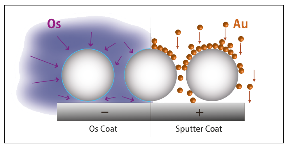
Os PE-CVD coating vs. Au Sputter coating
The results
General advantages of coating with osmium using plasma-enhanced chemical vapor deposition (PECVD):
- No charging
- No artifacts due to thermal effects
- Very fine grain size, original surface structure remains visible
Advantages at low magnifications
Acetatfaser
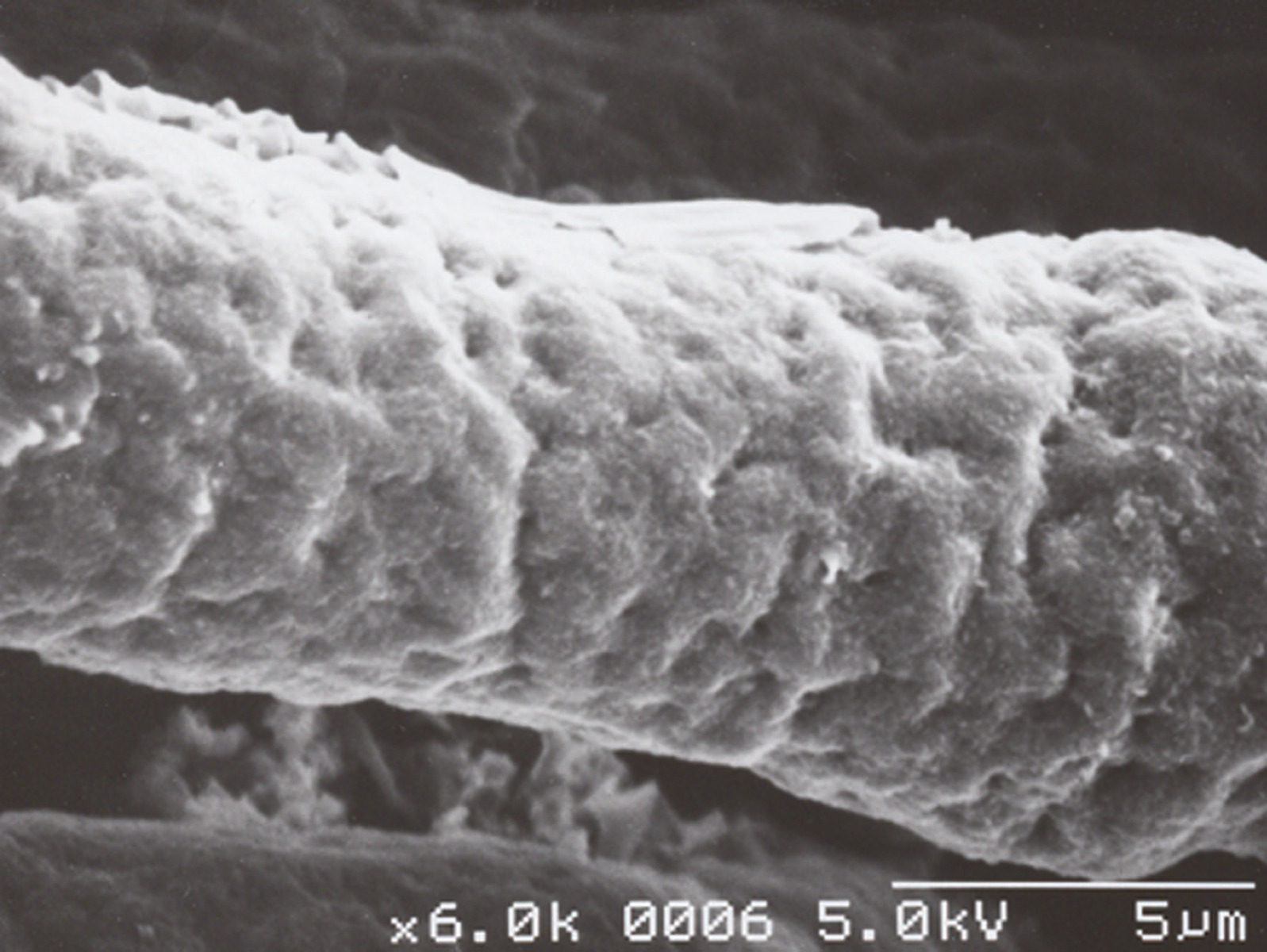
When sputtering with gold, charging effects occur due to the uneven distribution of the gold coating (right: metallic shimmering areas). The uniform coating with osmium prevents charging effects and the surface structure is retained (left). This difference is already visible at low magnification.
| Osmium-Coating | Gold-Sputter |
 |
 |
| Magnificaton: 500x | Magnification: 500x |
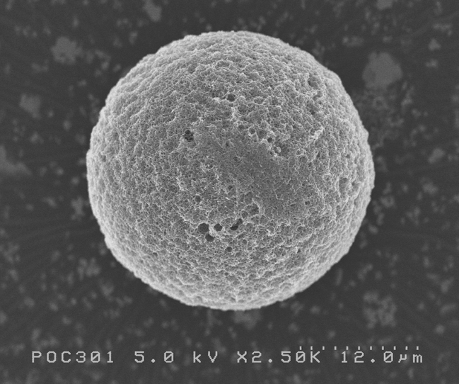
Polystyrene Particles
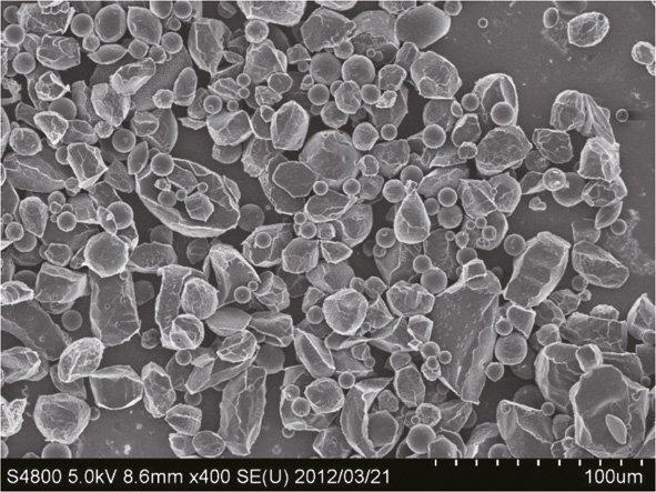
Charging especially in overlapping area of non-conducting particles is a common problem. The osmium coating is evenly distributed, even in the case of overlapping particles, so that an image acquisition with high contrast is possible without charging (top left). When sputtering with platinum, charging effects occur particularly at the particle overlap points due to insufficient coating (top right) due to shading. A higher magnification than 2,000x is not possible with a platinum coating due to charging (bottom right). The sample coated with osmium shows detailed structures without charging even at a magnification of 5,000x (bottom left).
| Osmium-Coating | Platinum-Coating |
 |
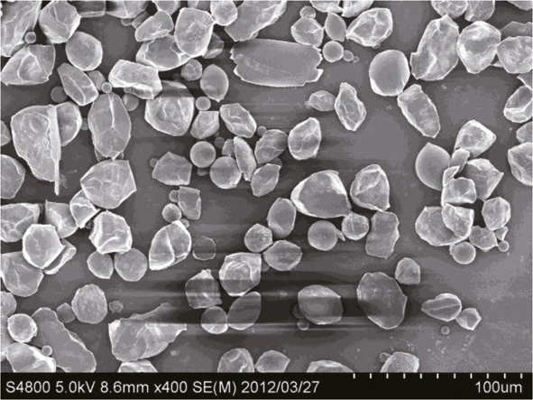 |
| Acceleration voltage: 5kV, Magnification: 400x | |
 |
 |
| Acceleration voltage: 5kV, Magnification: 5.000x | Acceleration voltage: 5kV, Magnification: 2.000x |
Data provided by: Hiroyuki Muto, Materials Electronics Division, Toyohashi University of Technology
Advantages at high Magnifications
- Even distribution of Osmium
- No accumulation compared to Sputter coating
- No loss of surface texture and structure
- No granularity at high magnification
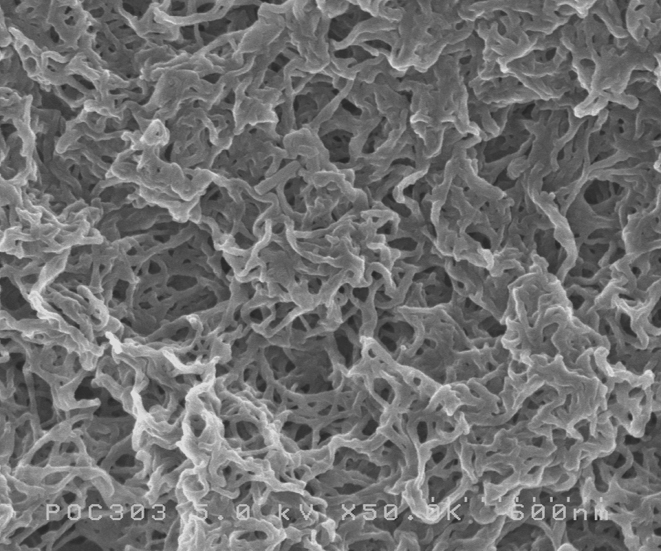
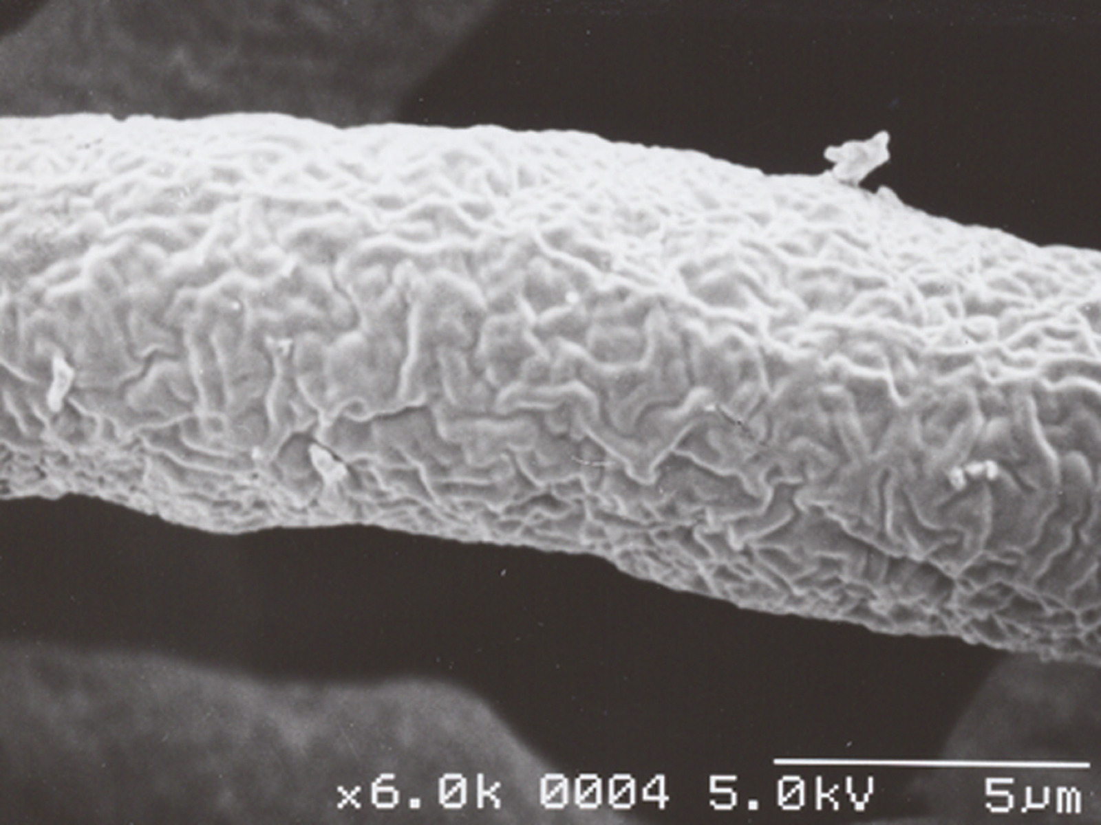
Polymer Film
At high magnification (100.000x) coating with Osmium still maintains the original surface integrity of the Polymer film sample (left). With platinum sputtering the original surface structure is hardly visible due to the high granularity and accumulation of platinum.
| Osmium-Coating | Platinum-Coating |
 |
 |
| Magnification: 100.000x | |
Data provided by: Industrial Technology Research Institute (ITRI), Taiwan
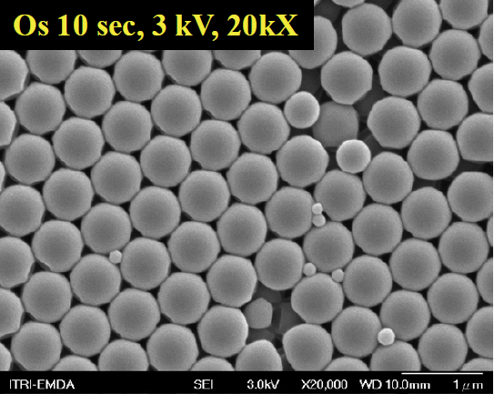
Polymer Beads
The electron beam causes significant damage to the surface of Platinum coated Polymer beads. However, beads coated with Osmium provide a clear image without any damage and charging
| Osmium-Coating |
Platinum-Coating |
 |
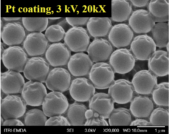 |
| Magnification: 20.000x | |
Data provided by: Industrial Technology Research Institute (ITRI), Taiwan
Protection of sensitive structures due to high melting point, good conductance and stability of Osmium: Great temperature and beam resistance
Carbon Nanotubes (CNT) at high magnification
The CNT structure collapses at higher magnifications in the gold (top right) and un-coated (top left) sample. Osmium coating (left) produces a reinforcing film to protect the sample from beam and heat damage enabling the imaging of CNT at magnifications of up to 40.000x. Even CNT contaminations of the SEM detectors are prevented by the osmium coating.
| Osmium-Coating | Gold-Sputter-Coating |
 |
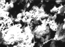 |
| Magnification: 40.000x | Magnification: 20.000x |
| Osmium-Coating | Uncoated |
 |
 |
| Magnification: 20.000x | Magnification: 20.000x |
Data provided by: Suzuki Tomoko, Ando Laboratory, Department of Materials and Functional Engineering, Faculty of Science and Technology, Meijo University
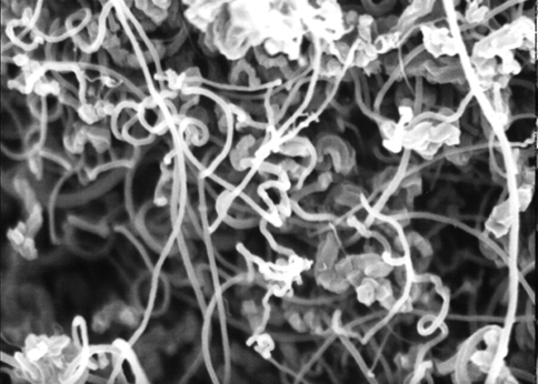
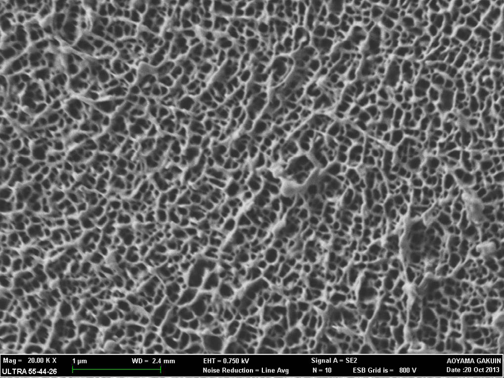
Lacewing Wings
The fine needle-like structure of the wing surface collapses in the uncoated sample (right). Whereas coating with Osmium maintains the structural integrity due to its protective properties (left).
| Osmium-Coating (3nm) | Uncoated |
 |
 |
|
Acceleration voltage: 0.75kV / Magnification: 20.000x |
|
Data provided by: Akito Takashima and Reona Takahashi, Faculty of Science and Engineering, Aoyama Gakuin University
Osmium Coating of complex Structures and Samples
- Even Coating Distribution
- No Shadowing
- Great visualization of deep structures
Conventional sputtering does not allow visualization of fine fiber meshes, cavities, rough surfaces or further complex structures due to incomplete coating efficiency. Osmium coatings allow detailed fine structures due its excellent isotropic coating making it possible to observe them at high magnifications.
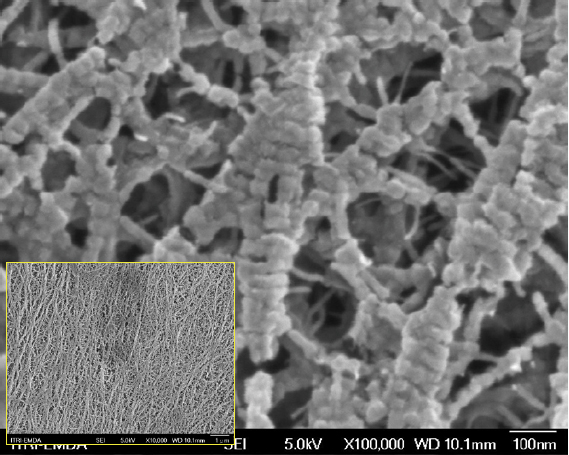
Cellulose Nanofibers (fine mesh-like structures)
| Osmium-Coating | ||
 |
 |
 |
| Acceleration voltage: 1,5kV /Magnification: 30.000x | Acceleration voltage: 1,5kV /Magnification: 60.000x | Acceleration voltage: 1,5kV /Magnification: 150.000x |
Data provided by: Seung-Hwan Lee, Biomass Research Center, National Institute of Advanced Industrial Science and Technology
Coal ash (rough surface, cavities and very fine structures)
| Osmium-Coating | |
 |
 |
| Magnification: 10.000x | Magnification: 150.000x |
Sepharose (crosslinked agarose bead with highly porous surface)
| Osmium-Coating | |
 |
 |
| Magnification: 2.500x | Magnification: 50.000x |
Star Sand the shell of Foraminifera (rough and porous surface, limestone)
| Osmium-Coating | |
 |
 |
| Magnification: 950x | Magnification: 10.000x |
Low deposition times for complex, fine and beam sensitive samples
No deformation or structural defects
Sputter coating takes about 3min to deposit enough Au or Pt on a complex structured sample. Thereby, samples shrink and are damaged by heat. The necessary high deposition time causes a swelling of structures and a loss of detail. Osmium coating takes only 20sec and deposits a thin and isotropic film without the generation of heat conserving the structure.
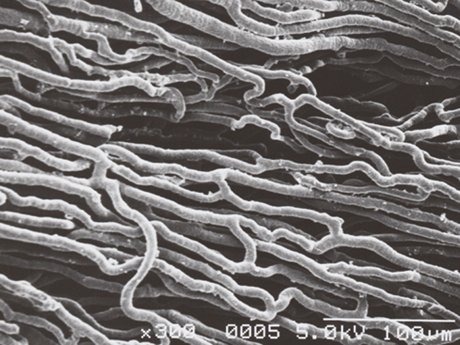
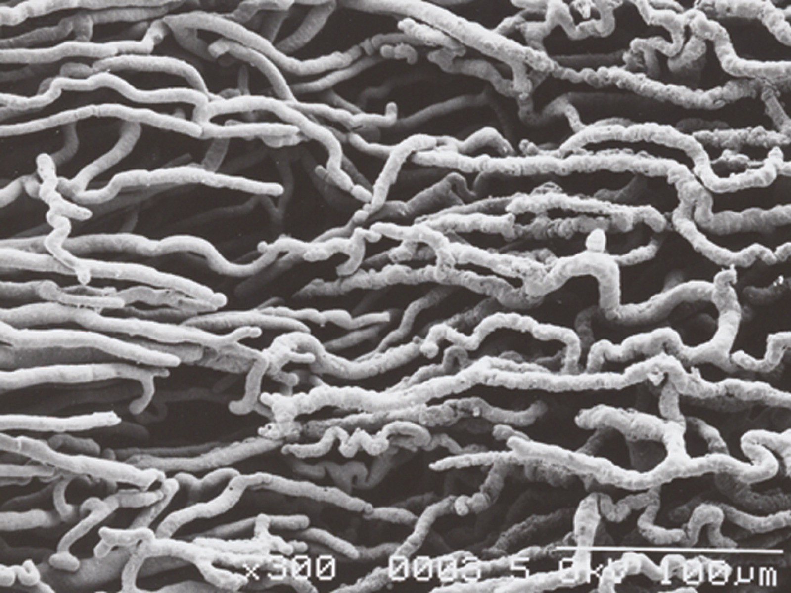
Replica of Rat cardiac blood Vessels
| Osmium-Coating (20 Sec.) | Gold-Sputter-Coating (3Min.) |
 |
 |
| Acceleration voltage: 5kV / Magnification: 300x | |
 |
 |
| Acceleration voltage: 5kV / Magnification: 6.000x | |
Data provided by: Okayama University Graduate School of Medicine, Dentistry, and Pharmaceutical Sciences, Department of Human Anatomy
More Information
| Manufacturer |
Meiwafosis
|
|---|---|
| Dimensions | 390(W) x 385(D) x 435(H)mm EN |
| Electrical Power | 230V |
| Packing Unit | each |
| Weight | 22kg |
| Weight | 0.000000 |
-
 €550.00 €654.50Art.Nr: BI76550
Precision machined from a block of aluminum – anodized black - this Sample Stub Vacuum Desiccators accommodates 18 SEM Mounted Sample Stubs, pin style, under vacuum for long time. Measures: 13x13cmx4,5cm. Chamber cavity is 10,4cm diameter x 18mm deep. Lid is made with 10mm thick clear acrylic.
€550.00 €654.50 -
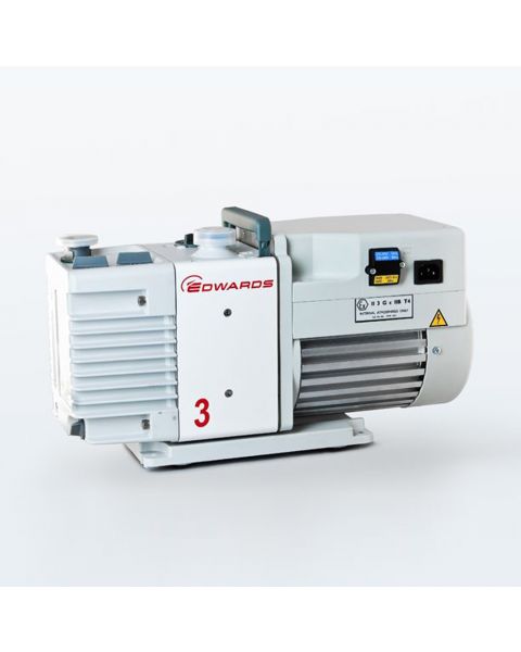
 €2,050.00 €2,439.50Art.Nr: ED91003
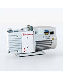
Edwards RV pumps have become the industry standard for scientific primary pumping applications. RV pumps are uniquely capable of delivering high or low throughputs with high ultimate vacuum. This, combined with ultra-low noise levels, makes them ideal for a wide range of applications including GCMS and other small bench top type applications. The RV3 has a suction capacity of 3.7 m³ / h (50 Hz).
Supplied with: 1 litre of Ultragrade 19 oil, inlet filter and O-ring.€2,050.00 €2,439.50 -
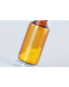
Starting at €58.40 €69.50
Small size (2ml), light-gauge, pre-scored amber glass ampoules. Ampoules containing OsO4 crystals are pre-cleaned and heat sealed in plastic bags to assure a contaminant-free solution.Starting at €58.40 €69.50
-

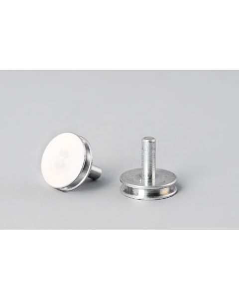
Starting at €3.40 €4.05
Made from pure aluminium. Lathe finish.Starting at €3.40 €4.05