Tennant20 Osmium Coating System for SEM
MFTE20
The Tennant20 Os-Coater is an advanced table-top PE-CVD system that creates high-quality pure conductive Os coatings for SEM sample preparation. The rotary pumped system creates ultra-thin coatings with very small grain-size and high conductivity.
Product Details
Description
Ultra-thin, conductive, metallic layers can be deposited very easily with the new Tennant20 Osmium Coater. It produces an isotropic, fine-grained coating ideal for non-conductive samples for SEM, EDX, EBSD, AES, XPS analysis.
The product name "Tennant20" derives from the name of the British scientist Smithson Tennant, who discovered Osmium in 1803. He isolated the metal along with iridium in residues of platinum dissolved in aqua regia.
The process:
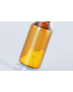
- Plasma-Enhanced-Chemical-Vapor-Deposition (PE-CVD) from OsO4-gas (sublimation source from OsO4 crystals)
>> more information on the coating process
The coating:
- Ultra-thin, conductive, pure Os films
- Very fine grain size
- No heat damage
- Isotropic coating
>> further information on the Os-coating
The results:
- Even on samples with a complicated structure, an Os film of 1-10nm thickness fully coats every side of the sample -> very few charging effects in the SEM
- Fine grain size preserves surface structure of samples at high resolution imaging
- Ultra-thin coatings <1nm show very low signal in EDX, AES, XPS, EBSD analysis
>> see example results obtained with Os-coating
The Osmium coating-process
The Tennant20 osmium coater uses a patented PE-CVD process (plasma-enhanced chemical vapor deposition) to create an ultra-thin yet conductive osmium film with a thickness of less than 1nm up to 30nm.
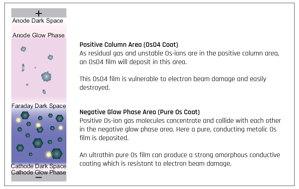
By the plasma CVD method, osmium tetroxide sublimation gas is introduced into the vacuum chamber and plasma is generated by DC glow discharge. During the process, the chamber is separated into two areas: „positive column“ and „negative glow phase“.
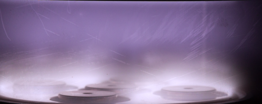
Source: Stefan Diller – Scientific Photography
Height of negative glow phase
The negative glow phase area of conventional electrodes is only 5mm high. An OsO4 coating is formed in the positive column area if a sample is taller than 5mm. The Tennant20 creates a larger negative glow phase area (20mm high) and larger samples can be coated in superior quality.
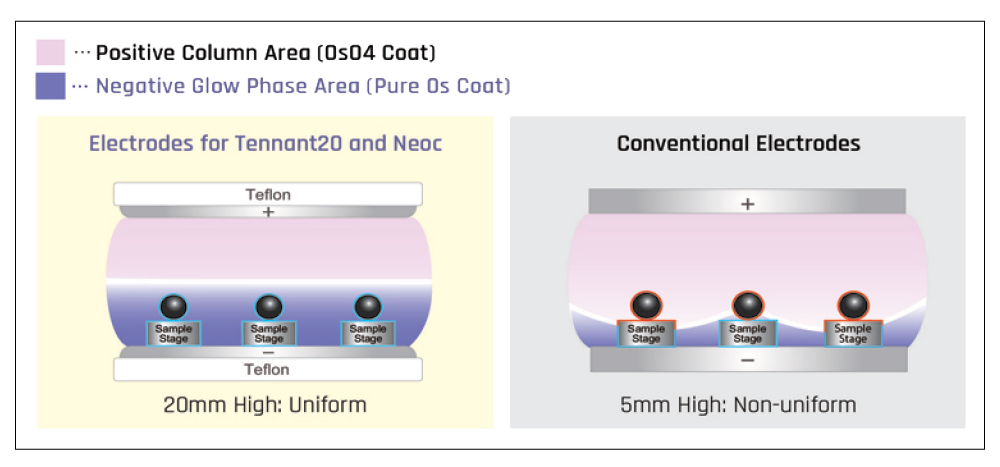
Uniform coating thickness
The coating thickness is non-uniform with conventional parallel plate type electrodes. It is thick at the center and the edge but it is thin in the center ring. The electrodes of the Tennant20 have a special design so that the discharge is not only centered on the edge but shows a uniform negative glow phase in the whole sample holding area.
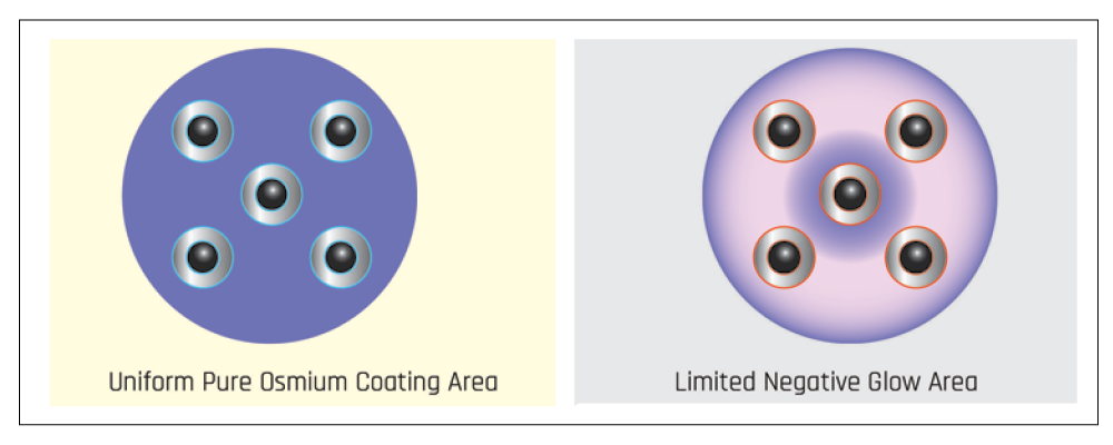
The Osmium film
Due to the coating process, the film is coated isotropically on all surfaces of the samples. Good conductivity is achieved even with complicated sample geometries such as three-dimensional biological samples, fibers, powder, porous materials or nanoparticles. The subsequent analyzes e.g. SEM, EDX, EBSD, AES, XPS are surprisingly successful, even at very high resolutions and beam intensities.
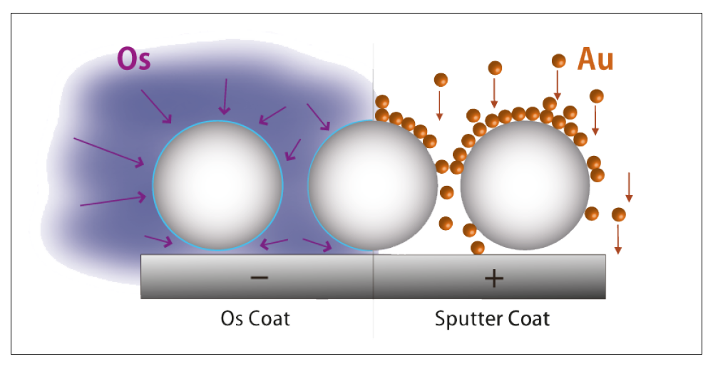
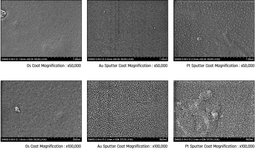
Os PE-CVD coating vs. Au Sputter coating
The results
Even samples which are usually difficult to image, as they are easily affected by charging and drifting, Os coating provides a clear image when it is purely coated in the negative glow phase area in the Tennant20 Os-coating system
Acetate Fiber
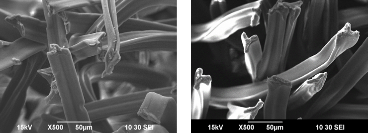
Os Coat Magnification : x500 / Au Sputter Coat Magnification : x500
The gold sputter coating shows imperfect surface coating and charges up. The texture of the surface looks metallic. With an osmium coating, the texture of the surface is clearly visible. Even at low magnifications, the different appearance of the surface layer is obvious.
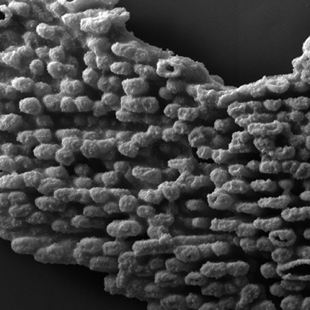
Green lacewing wings


Acceleration Voltage: 0,75kV / Magnification: 20.000x
This is an image of a lacewing wing observed with a low acceleration SEM. In uncoated images, the structure is affected and damaged by the electron beam. As a result, the original needle-like structure of the sample could not be observed. In contrast, the sample treated with an Os coating forms a strong conductive coating that is extremely resistant to electron beam damage. The original structure of the sample is not damaged and the needle-like structure can be clearly observed. In addition, as an osmium coating is hardly affected by heat, it is ideal for coating heat-sensitive resin materials and biological samples.
Image courtesy by Akito Takashima and Reona Takahashi, Faculty of Science and Engineering, Aoyama Gakuin University
SiC Wheel
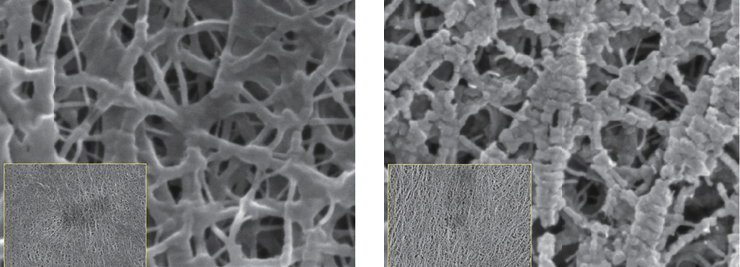
Polymer film, Osmium-coated, 100.000x Polymer film, Platinum-coated, 100.000x
Images by Industrial Technology Research Institute of Taiwan (ITRI)
A huge difference can be seen at a high magnification (x100,000). In the right image Pt has been sputtered on the sample and it is hard to see the original surface structure.
On the left side, no granularity is visible on the Os coated sample at high magnification. You can see the actual surface structure. Also Os coating does not cause heat damage to organic samples due to the low landing energies.
Data provided by The Industrial Technology Research Institute (ITRI)
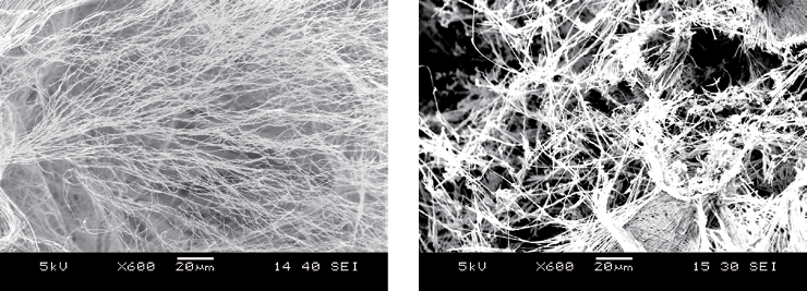
Freeze dried amino acid cake, Os-coated, 600x
Freeze-dried cake has a complicated matrix structure. It is easily blown up and susceptible to heat.
An Os coating provides a clear image of the original structure without any damage.
Freeze dried amino acid cake, Pt-coated
The network of the freezedried cake is blurred, the shadowed area and the depth are not clear.
The matrix structure gets crushed or fragmented by sputter particles.
Os Coating
Au/Pd Coating
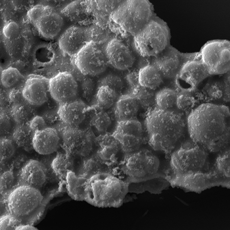
Microbes + 10nm
Os (SEM)
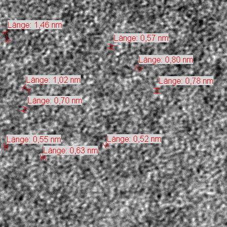
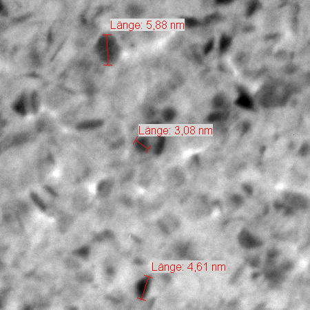
Particle Size
3nm Os on SiN
(TEM)
More Information
| Dimensions | 390(W) x 385(D) x 435(H)mm |
|---|---|
| Electrical Power | 230V |
| Packing Unit | each |
| Weight | 22kg |
| Weight | 22.000000 |

