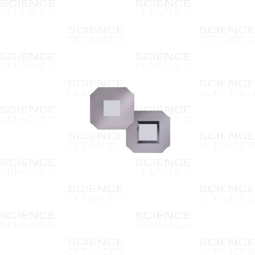
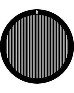
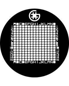
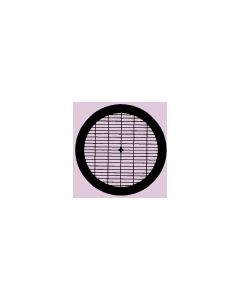
Continuous Silicon Nitride Film TEM Window Grids, single window
Silicon frames are 100µm thick. Grids fit standard 3mm holders and most double tilt holders.
Thicknesses available are 5, 10, 15, 20, 30, 50, 100 and 200 nm, window sizes are squares of 0,01mm, 0,025, 0,05, 0,1, 0,15, 0,25, 0,5, 1mm or arrays.
Product Details
Description
Features
- Plasma Cleanable - can be vigorously plasma cleaned to remove organic contamination
- High Temperature Tolerance - resist temperatures up to and above 1000°C
- Mechanical Robustness - withstand harsh conditions
- Flat, insulating and hydrophobic - incorporates LPCVD, low-stress(~250MPa), non-stoichiometric silicon nitride
- Chemically Inert - resistant to bases, acids (except HF) and solvents
- High Beam Current Tolerant
- Carbon-Free and Ultra-Clean
- Good X-ray transmission performance
- Compatible - fit standard 3mm TEM grid holders, octagonal shape
Uses:
- Environmental TEM (dynamic processes at high temperatures)
- Nanoparticle imaging
- Analysis of nano materials, semiconductor materials, optic-crystal materials, functional film materials etc.
- (Quantitative) Carbon Analysis (photoresist, polymers, food, oil, fuel etc.)
- Crystal growth research
- X-Ray microscopy and X-Ray spectroscopy techniques
- Thin film research
- In-situ characterization of chemical reactions and annealing effects
- Biological sample observation thanks to superior biocompatibility: on-film growth of cells or other biological samples
- Characterization experiments of colloids, aerogels, organic materials and nanoparticles
Recommended Use
| SiN film thickness | Product examples and window sizes | |
|
Highest Resolution Imaging |
5nm | E76042-43, 1 square (0,025mm) E76042-44, 8 squares (0,05mm), 1 slot (0,05x0,1mm) E76042-45, 2 slots (0,05x1,5mm)* |
| High Resolution | 10nm | E76042-46, 8 squares (0,1mm), 1 slot (0,1x0,35mm) E76042-47, 8 squares (0,25mm), 1 slot (0,25x0,5mm) YSG010Z, 1 square (0,1mm) YSG015Z, 1 square (0,15mm) YSG025Z, 1 square (0,25mm) YSG050Z, 1 square (0,5mm) YSAR010Z, 9 squares (0,1mm) |
| Everyday Imaging | 20nm | YSG001AT, 1 square (0,01mm) E76042-48, 8 squares (0,1mm), 1 slot (0,1x0,35mm) E76042-49, 1 square (0,5mm) E76042-50, 9 squares (0,1mm) |
| Demanding Conditions | 50nm | E76042-53, 1 square (0,1mm) E76042-52, 1 square (0,5mm) E76042-51, 1 square (1mm) YSTA015C, 2 slots (0,1x1,5mm) E76042-50, 9 squares (0,1mm) |
| Suspension Materials & Cryo-TEM | Microporös, nanoporös | E76042-41, 1 square (0,5mm) E76042-40, 1 square (0,5mm) YSME050B, 1 square (0,5mm), 2,8μm holes YSME050C, 1 square (0,5mm), 2,0μm holes YSME050C10, 1 square (0,5mm), 10μm holes YSME050E05, 1 square (0,5mm), 5μm holes YSNP-TE025B, 1 square (0,25mm), 20-200nm holes, 50nm SiN YSNP-TE010D, 1 square (0,1mm), 20-200nm holes, 200nm SiN |
*Coated with 1nm ultrahigh purity carbon to minimize charging
More Information
| Film Type |
Continuous SiN film
|
|---|---|
| Material |
Silicon Nitride
|

